- 您现在的位置:买卖IC网 > Sheet目录1902 > AT32UC3C2512C-A2UT (Atmel)IC MCU AVR32 512K FLASH 64TQFP
67
32117DS–AVR-01/12
AT32UC3C
Note:
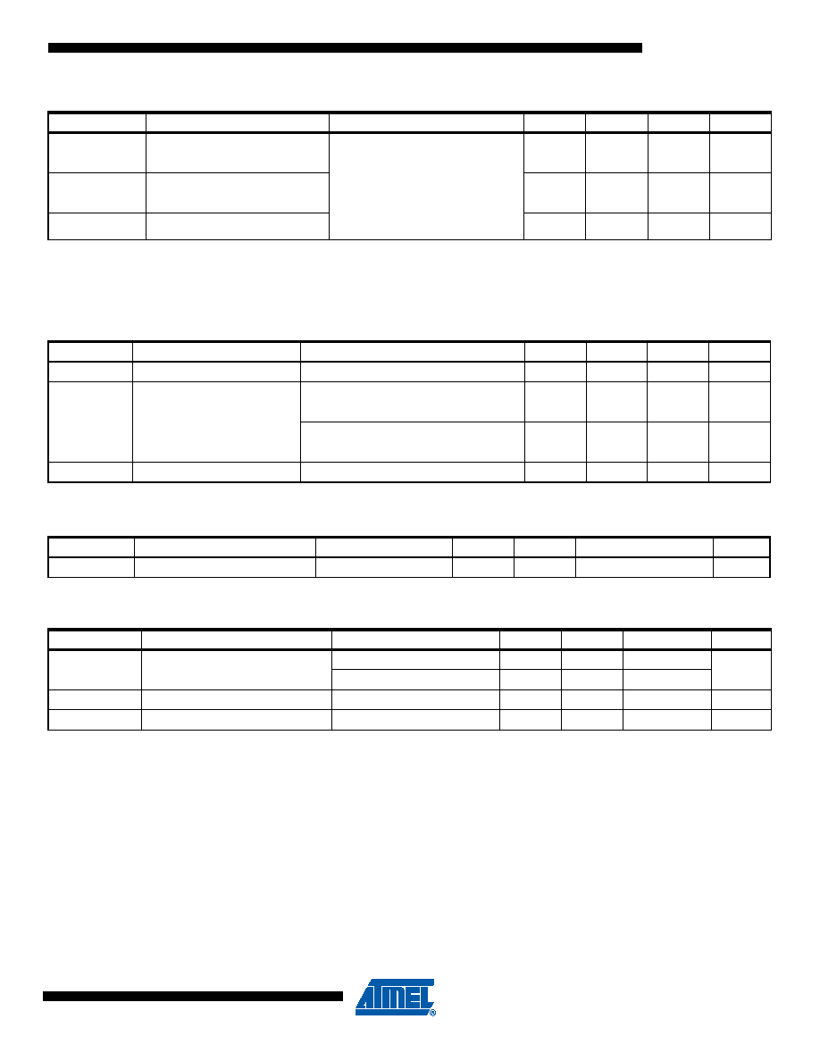
1. The measures are done without any I/O activity on VDDANA/GNDANA power domain.
7.8.7
Digital to Analog Converter (DAC) Characteristics
RES
Resolution
Differential mode,
V
VDDANA = 5V,
VADCREF0 = 3V,
ADCFIA.SEQCFGn.SRES = 1,
S/H gain from 1 to 16
(Fadc = 1.5MHz)
10
Bit
INL
Integral Non-Linearity
1.5
LSB
DNL
Differential Non-Linearity
1.5
LSB
Offset error
-25
25
mV
Gain error
-15
15
mV
Table 7-36.
ADC and S/H Transfer Characteristics (Continued)10-bit Resolution Mode and S/H gain from 1 to 16(1)
Symbol
Parameter
Conditions
Min
Typ
Max
Units
Table 7-37.
Channel Conversion Time and DAC Clock
Symbol
Parameter
Conditions
Min
Typ
Max
Units
fDAC
DAC clock frequency
1MHz
tSTARTUP
Startup time
3s
tCONV
Conversion time (latency)
No S/H enabled, internal DAC
1
s
One S/H
1.5
s
Two S/H
2
s
Throughput rate
1/tCONV
MSPS
Table 7-38.
External Voltage Reference Input
Symbol
Parameter
Conditions
Min
Typ
Max
Units
V
DACREF
DACREF input voltage range
1.2
V
VDDANA-0.7
V
Table 7-39.
DAC Outputs
Symbol
Parameter
Conditions
Min
Typ
Max
Units
Output range
with external DAC reference
0.2
V
DACREF
V
with internal DAC reference
0.2
V
VDDANA-0.7
C
LOAD
Output capacitance
0
100
pF
R
LOAD
Output resitance
2
k
Ω
发布紧急采购,3分钟左右您将得到回复。
相关PDF资料
AT32UC3C2512C-A2ZT
IC MCU 32BIT 512KB FLASH 64TQFP
AT32UC3L016-D3HR
MCU AVR32 16K FLASH 48TTLGA
AT42QT5480-CU QS444
IC SENSOR DUAL TOUCH 49-BGA
AT6010H-4QI
IC FPGA 4NS 240PQFP
AT80C31X2-SLRUM
MCU ROMLESS 31X2 5V 44-PLCC
AT80C51RD2-SLRUM
IC MCU 80C51 HI PERFORM 44PLCC
AT85C51SND3B1-RTTUL
IC DECODER/ENCODER DGTL 100-LQFP
AT87251G2D-RLTUM
IC MCU 8/16BIT 32K OTP 44-VQFP
相关代理商/技术参数
AT32UC3C2512C-A2ZR
功能描述:32位微控制器 - MCU 512KB FL,-40/125oC AUTO
RoHS:否 制造商:Texas Instruments 核心:C28x 处理器系列:TMS320F28x 数据总线宽度:32 bit 最大时钟频率:90 MHz 程序存储器大小:64 KB 数据 RAM 大小:26 KB 片上 ADC:Yes 工作电源电压:2.97 V to 3.63 V 工作温度范围:- 40 C to + 105 C 封装 / 箱体:LQFP-80 安装风格:SMD/SMT
AT32UC3C2512C-A2ZT
功能描述:32位微控制器 - MCU 512KB FL,-40/125oC AUTO
RoHS:否 制造商:Texas Instruments 核心:C28x 处理器系列:TMS320F28x 数据总线宽度:32 bit 最大时钟频率:90 MHz 程序存储器大小:64 KB 数据 RAM 大小:26 KB 片上 ADC:Yes 工作电源电压:2.97 V to 3.63 V 工作温度范围:- 40 C to + 105 C 封装 / 箱体:LQFP-80 安装风格:SMD/SMT
AT32UC3C2512C-Z2UR
制造商:Atmel Corporation 功能描述:MCU 32-bit AT32 AVR RISC 512KB Flash 3.3V/5V 64-Pin QFN EP T/R 制造商:Atmel Corporation 功能描述:512KB FLASH 64QFN(-40?C TO 85?C) T&R - Tape and Reel 制造商:Atmel Corporation 功能描述:IC MCU 32BIT 512KB FLASH 64QFN 制造商:Atmel Corporation 功能描述:32-bit Microcontrollers - MCU 512KB Flash 64QFN (-40oC to 85oC) 制造商:Atmel Corporation 功能描述:512KB Flash 64QFN(-40C to 85C) T&R
AT32UC3C2512C-Z2UT
制造商:Atmel Corporation 功能描述:512KFLASH AUTO - Trays
AT32UC3C2512C-Z2ZES
制造商:Atmel Corporation 功能描述:512KFLASH UC3C AUTO - QFN64 ENG SAMPLE - Bulk
AT32UC3C2512C-Z2ZR
功能描述:32位微控制器 - MCU 512KB FL,-40/125oC AUTO
RoHS:否 制造商:Texas Instruments 核心:C28x 处理器系列:TMS320F28x 数据总线宽度:32 bit 最大时钟频率:90 MHz 程序存储器大小:64 KB 数据 RAM 大小:26 KB 片上 ADC:Yes 工作电源电压:2.97 V to 3.63 V 工作温度范围:- 40 C to + 105 C 封装 / 箱体:LQFP-80 安装风格:SMD/SMT
AT32UC3C2512C-Z2ZT
功能描述:32位微控制器 - MCU 512KB FL,-40/125oC AUTO
RoHS:否 制造商:Texas Instruments 核心:C28x 处理器系列:TMS320F28x 数据总线宽度:32 bit 最大时钟频率:90 MHz 程序存储器大小:64 KB 数据 RAM 大小:26 KB 片上 ADC:Yes 工作电源电压:2.97 V to 3.63 V 工作温度范围:- 40 C to + 105 C 封装 / 箱体:LQFP-80 安装风格:SMD/SMT
AT32UC3C264C-A2UR
功能描述:32位微控制器 - MCU UC3C 64K FLASH 16K SRAM
RoHS:否 制造商:Texas Instruments 核心:C28x 处理器系列:TMS320F28x 数据总线宽度:32 bit 最大时钟频率:90 MHz 程序存储器大小:64 KB 数据 RAM 大小:26 KB 片上 ADC:Yes 工作电源电压:2.97 V to 3.63 V 工作温度范围:- 40 C to + 105 C 封装 / 箱体:LQFP-80 安装风格:SMD/SMT